From Transistors to Gates and Functions
For the purpose of this class, we will consider transistors to be the basic building blocks of computer hardware.
A transistor is an electronic device that has three ends: a source, a sink, and a gate. The figure below shows three individual transistors (circa 1960s). Today's technology allows us to pack up to 1 million transistors per square millimeter (circa 2006). An Intel processor measuring less than a square inch has well over 1.5 billion transistors on it (circa 2007) -- more data available here.
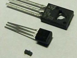
Figure 1: Picture of individual transistors (courtesy of Wikipedia).
More conveniently, transistors are depicted using the picture below.
Figure 2: Symbol used to depict a transistor with its three connection points.
Transistors as Faucets!
The operation of a transistor could be explained by making an analogy to faucets.
Just like a transistor, a faucet is connected to a source (the water company), the faucet drains in a sink, and the flow of water through the faucet is controlled by a gate (the knob). If the faucet knob (gate) is turned ON water flows from the source to the sink, otherwise if the faucet knob (gate) is turned OFF no water flows.
Figure 3: Faucet Operation: The gate controls the flow of water from source to sink.
If we represent the fact that water flows from the source to the sink with a 1 (or ON) and the fact that water does not flow from the source to the sink with a 0 (or OFF), we can understand how a transistor works simply by changing "water" to "electricity". In particular:
-
When the gate of a transistor is ON (or has a value 1) then electricity flows from the source to the sink and the transistor is said to be ON
-
Otherwise when the gate of a transistor is OFF (or has a value 0) then electricity does not flow from the source to the sink and the transistor is said to be OFF.
The current technology used to build computer hardware (chips) is called CMOS, which stands for Complementary Metal–Oxide–Semiconductor.
In CMOS, in addition to using the transistor described above, we use another kind of transistors, which is turned ON when the gate is OFF and is turned OFF when the gate is ON. In other words, its operation is "complementary" (or opposite) to the one we just described above. The symbol for this complementary type of transistors is shown below. The symbol is quite similar to the transistor we described above, except for the "bubble" connected to the gate. This bubble means that this transistor works in the opposite way (it's ON when the gate is OFF and OFF when the gate is ON.
Figure 4: Symbol used to depict a complementary transistor.
To carry the analogy with faucets, one can think of a faucet that lets water flow from the source to the sink when its knob is tightened but not when the knob is loosened.
Using Transistors to Build Bigger Circuits
Using transistors as building blocks, we can build larger circuits that perform interesting (logical) operations.
Our first example is the NOT circuit. The figure below shows how to connect two transistors together to build an inverter (also known as a NOT gate).
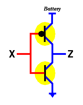
Figure 5: An inverter circuit (known as the NOT gate).
Now, let's find out what the inverter circuit above will do when presented with an input (i.e. X). We know that X can take one of two values, either 0 or 1. Let's study each one separately.
-
If X=0 then by definition of the bottom transistor, it will be OFF, which means that electricity will not be able to flow from its source to its sink. Also, by definition, the top transistor will be ON, which means that electricity will be able to flow from its source to its sink. The question is, will there be any electricity coming out from Z (where Z is the output of that circuit). The answer is YES. Since the top transistor is ON and the bottom transistor is OFF, electricity flowing out of the battery will go through the top transistor but will not be able to make it through the bottom one. In other words, it will flow out through Z. To visualize the operation of the inverter, it may be helpful to think about this example using the water analogy discussed before.
-
If X=1 then by definition of the bottom transistor, it will be ON, which means that any electricity already available at its source will drain in the sink. Also, by definition, the top transistor will be OFF, which means that no electricity will be able to flow from its source to its sink. The question is, will there be any electricity coming out from Z (where Z is the output of that circuit). The answer is NO. Since the top transistor is OFF and the bottom transistor is ON, electricity flowing out of the battery will be blocked by the top transistor and any electricity that may exist in Z, will drain. In other words, there will be no electricity flowing out through Z. Again, it may be helpful to think about this example using the water analogy discussed before.
The table below sums up the operation of the NOT gate by providing an output (Z) for every possible input (X) of the circuit. Tables like this one (providing us with the value of a function for all possible combination of inputs of that function) are called truth tables.
|
NOT
|
The figure below shows how one could build another circuit using transistors. This circuit has two inputs X and Y and one output Z.
There are 4 possibilities for the inputs, namely
- X=0, Y=0
- X=0, Y=1
- X=1, Y=0
- X=1, Y=1
Let's try to do an analysis similar to what we did for the NOT gate. In particular, consider the case when both X and Y are 0. By definition, the bottom two transistors will be OFF while the top two will be ON thus allowing electricity to flow from the battery to the output Z. Thus for X=0, Y=0 we get Z=1. In the case when both X and Y are 1, the bottom two transistors will be ON while the top two will be OFF, thus no electricity will flow from the battery to the output Z. Thus for X=1, Y=1 we get Z=0. In the case when X=0 and Y=1, we notice that one of the two top transistors will be ON and the other will be OFF. Similarly, for the bottom transistors, one will be ON and the other will be OFF. Thus, electricity will still be able to flow to Z (through the ON transistor on top), thus making Z=1. The case for X=1, Y=0 is similar. It yields Z=1.
Thus we get the truth table below for the circuit shown above.
|
NAND
|
The above truth table says that the output of the circuit is 0 only when the two inputs are 1 this is exactly the opposite of the AND logical function (the AND logical function outputs 1 whenever both its first input AND its second input are 1). Thus we call this circuit the "Not AND" gate or the NAND gate.
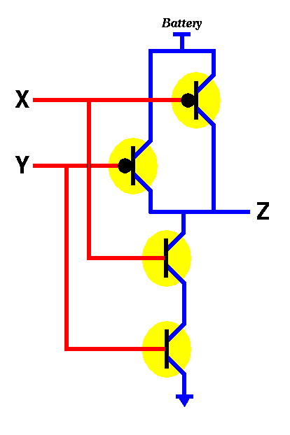
In order to build an AND gate, all we have to do is to connect the output of the NAND gate to the input of a NOT gate.
 |
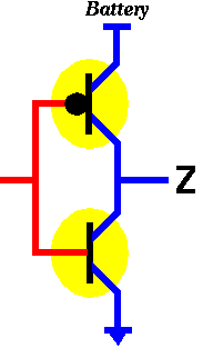 |
Figure 9: The "both X and Y" circuit (the AND function).
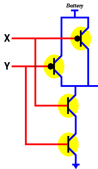
Similar to the NAND gate we can build a NOR (Not OR) gate as shown in the figure below.
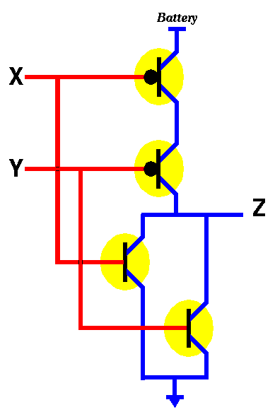
Figure 10: The "not X nor Y" circuit (the NOR function).
We leave it as an exercise to check that the truth table for the above circuit is as shown below.
|
NOR
|
Basic Logic Functions
From the above examples and discussion, we conclude that we can construct the main logic functions AND, OR, and NOT using transistors.
Since we will be using these functions (or gates) in future designs, we will give them symbols so that we don't have to draw all the transistors and all the connections each time we want to use (say) an OR gate.
For an OR gate we will use the symbol below:
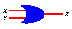
|
OR
|
Figure 12: Symbol of an OR gate and its truth table.
For an AND gate we will use the symbol below:
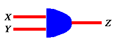
|
AND
|
Figure 13: Symbol of an AND gate and its truth table.
Finally, for the NOT gate we will use the symbol below:
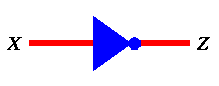
|
NOT
|
Figure 14: Symbol of a NOT gate and its truth table.
Other Logic Functions
By putting AND, OR, and NOT gates together, we can construct more complex (logic) functions.
Let's start with the simple example shown in the figure below-- namely, constructing a three-input OR gate out of two-input OR gates. Notice that the behavior of the three-input OR gate is to produce an output of 1 when at least one of the inputs is 1, otherwise (i.e. when all inputs are 0, it produces 0).
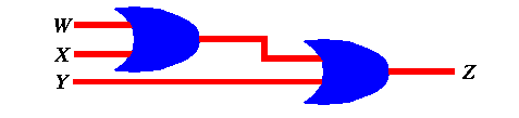
Figure 15: A 3-input OR function constructed using two 2-input OR gates.
This process could be generalized thus allowing us to build four-input, five-input, etc.. OR gates.
Similarly, we can also construct AND gates with more than two inputs. For example the figure below shows two different ways of implementing a 4-input AND gate from 2-input AND gates.
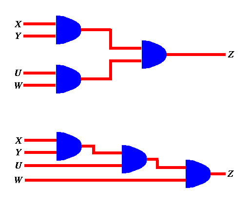
Figure 16: A 4-input AND function constructed using three 2-input AND gates.
The above two examples are simple, since one can predict the behavior of many AND gates connected together or the behavior of many OR gates connected together. Generally speaking, however, this may not be that simple. Given an arbitrary circuit, we can find out what it does by constructing its truth table , which is a tabulation of the circuit output for all possible input combinations. Take for example the circuit below.
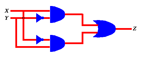
Figure 17: A function constructed by connecting various AND, OR, and NOT gates.
First, we notice that it has two inputs, X and Y. Each one of these inputs may assume one of two values 0 and 1. Thus the truth table for that circuit will have four entries. For each such entry we have to find out the output Z. We do so by labeling the circuit.
For example, if X = 0 and Y = 0 , we can label the various inputs and outputs of all gates until we find out that Z = 0 as shown below.
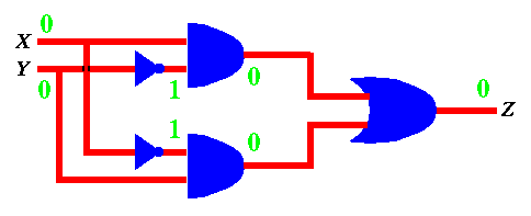
Figure 18: Output of function in Figure 15 when X=0 and Y=0.
Similarly, we can do it for X = 0 and Y = 1 to get Z = 1 as shown below.
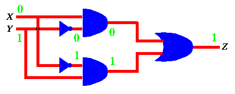
Figure 19: Output of function in Figure 15 when X=0 and Y=1.
If we do this for all 4 input combinations, we get the truth table below.
|
XOR
|
Figure 20: Truth table for function in Figure 17 -- function is known as XOR.
Notice that the above procedure could be used to find out the truth table for any logical circuit.
From the truth table in Figure 20, we notice that the behavior of the circuit is such that it produces an output of 1 if both inputs are not the same --i.e., when either one of its inputs is 1 but not both. This function is called the exclusive or (XOR) function. The figure below shows the symbol used to depict the XOR function (or gate) shown in Figure 17.
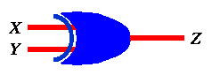
Figure 21: Symbol of XOR gate.
Can you guess how many transistors it would take to build the above XOR gate?
To summarize, if we take transistors as a building block, one can see how to combine a handful of transistors to build logical functions such as AND, OR, NOT, XOR, etc. By putting a few of these together we get even more complex (interesting) functions, and the process goes on, allowing us to build functionalities as complex as those supported by (say) the processor in your PC.