CLA CS-101: Introduction to Computers
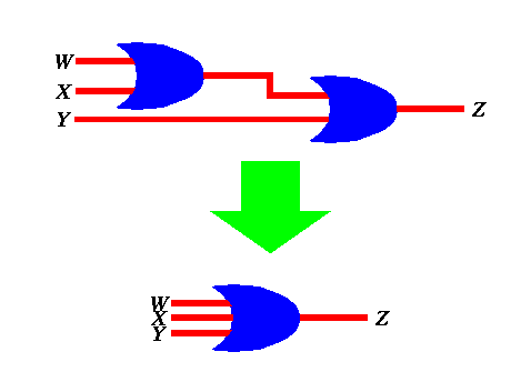
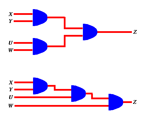
The above could be also done for AND gates. For example the figure below shows two different ways of implementing a 4-input AND gate from 2-input AND gates.
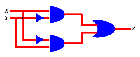
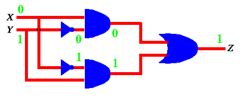
First, we notice that it has two inputs, X and Y. Each one of these inputs may assume one of two values 0 and 1. Thus the truth table for that circuit will have four entries. For each such entry we have to find out the output Z. We do so by labeling the circuit. For example, if X = 0 and Y = 0 , we can label the various inputs and outputs of all gates until we find out that Z = 0 as shown below...
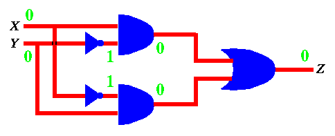
Similarily, we can do it for X = 0 and Y = 1 to get Z = 1 as shown below...
If we do this for all 4 input combinations, we get the truth table below.
  XOR --------------
     |  X  Y  |  Z  |
     | -------+-----
     |  0  0  |  0  |
     |  0  1  |  1  |
     |  1  0  |  1  |
     |  1  1  |  0  |
      --------------
The above procedure for finding out what the truth table for a particular circuit is could be repeated for any circuit.
First, one has to identify all the "rows" in the truth table for which the output is a 1. Each one of these rows identifies a combination of inputs for which the output must be 1. Thus, one may say that the output must be 1 if the first such combination is present, or the second is present, or the third is present, etc... Thus the output of this circuit is the output of an OR gate whose inputs are the outputs of a number of smaller sub-circuits, each corresponding to a given row in the truth table with an output of 1 .
Second, for each row in the truth table (and thus for every sub-circuit connected to the OR gate), we notice that a particular pattern for the inputs must be present. Such a pattern can be tested using an AND gate with as many inputs as there are inputs to the truth table. A particular input to the AND gate is inverted (using a NOT gate) if its corresponding input in the truth table is 0.
Let's look at an example... Assume we want to build a circuit that has three binary inputs W, X, and Y and one output Z, which is to be 1 when all three inputs are identical (i.e. all 0 or all 1). The tuth table for such a circuit is shown below.
Majority -----------------
        |  W  X  Y  |  Z  |
        | ----------+-----
        |  0  0  0  |  1  |
        |  0  0  1  |  0  |
        |  0  1  0  |  0  |
        |  0  1  1  |  0  |
        |  1  0  0  |  0  |
        |  1  0  1  |  0  |
        |  1  1  0  |  0  |
        |  1  1  1  |  1  |
         -----------------
[To be continued...]
Created on: April 13, 1995.
Updated on: April 12, 1995.