CLA CS-101: Introduction to Computers
The operation of a transistor could be explained by making an analogy to faucets. A faucet is connected to a source (the water company) and a sink (where water is drained). If the tap knob (gate) is turned ON water flows from the source to the sink, otherwise if the tap knob (gate) is turned OFF no water flows.
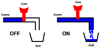
If we represent the fact that water flows from the source to the sink with a 1 (or ON) and the fact that water does not flow from the source to the sink with a 0 (or OFF), we can understand how a transistor works simply by changing "water" to "electricity". In particular, when the gate of a transistor is ON (or has a value 1) then electricity flows from the source to the sink and the transistor is said to be ON, otherwise when the gate of a transistor is OFF (or has a value 0) then electricity does not flow from the source to the sink and the transistor is said to be OFF.
The current technology used to build computer hardware (chips) is called CMOS. In CMOS, in addition to using the transistor described above, we use another kind of transistors, which is turned ON when the gate is OFF and is turned OFF when the gate is ON. The symbol for this kind of transistors is shown below. It is quite similar to the transistor we described above, except for the "bubble" connected to the gate. This bubble means that this transistor works in the opposite way (it's ON when the gate is OFF and OFF when the gate is ON).
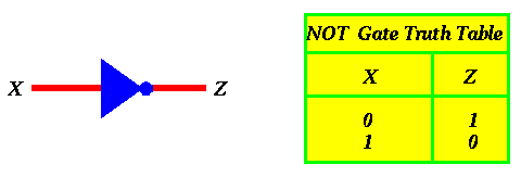
Our first example is the NOT circuit. The figure below shows how to connect two transistors together to build an inverter (also known as a NOT gate).
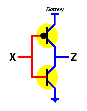
Now, let's find out what the inverter circuit above will do when the input to it (i.e. X) changes. We know that X can take one of two values, either 0 or 1. Let's study each one separately.
If X=0 then by definition of the bottom transistor, it will be OFF, which means that electricity will not be able to flow from its source to its sink. Also, by definition, the top transistor will be ON, which means that electricity will be able to flow from its source to its sink. The question is, will there be any electricity coming out from Z (where Z is the output of that circuit). The answer is YES. Since the top transistor is ON and the bottom transistor is OFF, electricity flowing out of the battery will go through the top transistor but will not be able to make it through the bottom one. In other words, it will flow out through Z. Again, it may be helpful to think about this example using the water analogy discussed before.
If X=1 then by definition of the bottom transistor, it will be ON, which means that any electricity already available at its source will drain in the sink. Also, by definition, the top transistor will be OFF, which means that no electricity will be able to flow from its source to its sink. The question is, will there be any electricity coming out from Z (where Z is the output of that circuit). The answer is NO. Since the top transistor is OFF and the bottom transistor is ON, electricity flowing out of the battery will be blocked by the top transistor and any electricity that may exist in Z, will drain. In other words, there will be no electricity flowing out through Z. Again, it may be helpful to think about this example using the water analogy discussed before.
Thus, to sum up the operation of this circuit, we present its truth table below:
  NOT -----------
     |  X  |  Z  |
     | ----+-----
     |  0  |  1  |
     |  1  |  0  |
      -----------
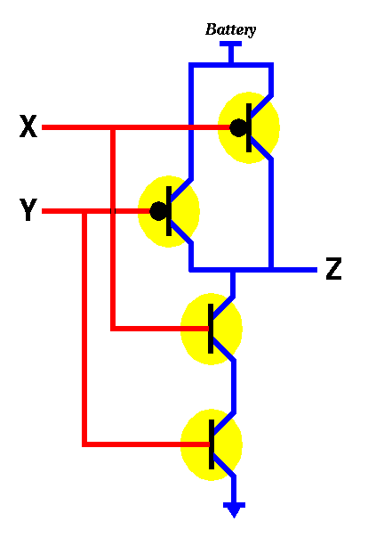
There are 4 possibilities for the inputs, namely X=0, Y=0; X=0, Y=1; X=1, Y=0; and X=1, Y=1. Let's try to do an analysis similar to what we did for the NOT gate. In particular, consider the case when both X and Y are 0. By definition, the bottom two transistors will be OFF while the top two will be ON thus allowing electricity to flow from the battery to the output Z. Thus for X=0, Y=0 we get Z=1. In the case when both X and Y are 1, the bottom two transistors will be ON while the top two will be OFF, thus no electricity will flow from the battery to the output Z. Thus for X=1, Y=1 we get Z=0. In the case when X=0 and Y=1, we notice that one of the two top transistors will be ON and the other will be OFF. Similarily, for the bottom transistors, one will be ON and the other will be OFF. Thus, electricity will still be able to flow to Z (through the ON transistor on top), thus making Z=1. The case for X=1, Y=0 is similar. It yields Z=1. Thus we get the truth table below...
 NAND --------------
     |  X  Y  |  Z  |
     | -------+-----
     |  0  0  |  1  |
     |  0  1  |  1  |
     |  1  0  |  1  |
     |  1  1  |  0  |
      --------------
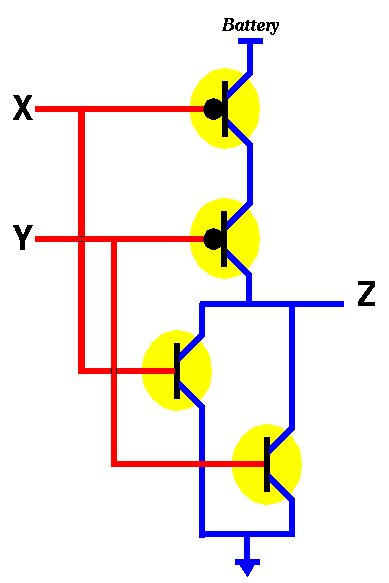
We leave as an exercice to check that the truth table for the above circuit is as shown below.
  NOR --------------
     |  X  Y  |  Z  |
     | -------+-----
     |  0  0  |  1  |
     |  0  1  |  0  |
     |  1  0  |  0  |
     |  1  1  |  0  |
      --------------
Since we will be using these gates in future designs, we will give them symbols so that we don't have to draw all the transistors and all the connections each time we want to use (say) an OR gate...
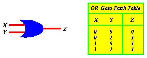
For an OR gate we will use the symbol below:
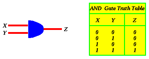
For an AND gate we will use the symbol below:
Finally, for the NOT gate we will use the symbol below:
Created on: April 12, 1995.
Updated on: April 12, 1995.